锗晶圆

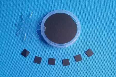
高纯锗晶圆具有优异的载流子迁移率和红外透过率,广泛应用于红外光学器件、太阳能电池、半导体器件及光电探测领域。

描述

锗晶圆先进技术:苏州科跃材料科技有限公司的专业承诺

苏州科跃材料科技有限公司提供高纯度锗(Ge)晶圆,具有优异的载流子迁移率、直接带隙特性以及出色的红外透过性能。这些晶圆广泛应用于半导体、光子学以及红外(IR)光学领域,是高性能晶体管、太阳能电池和热成像系统的理想选择。

锗晶圆与III-V族材料之间晶格失配较小,有利于实现高质量的外延生长,适用于先进的光电器件。其高折射率与优异的红外透过率,使其成为红外光学和传感技术中的首选材料。此外,锗晶圆也广泛应用于异质结双极型晶体管(HBT)以及兼容CMOS工艺的半导体器件中。

苏州科跃材料科技有限公司可根据客户需求,定制不同尺寸、掺杂类型和技术参数的锗晶圆,以满足科研与工业领域的多样化应用,确保材料品质与器件性能的卓越表现。


锗晶圆规格参数

  • 尺寸:10×3,10×5,10×10,15×15,20×15,20×20,直径1″、2″、4″、6″

  • 厚度:0.33mm,0.43mm,0.5mm,1.0mm

  • 表面处理:单面抛光(SSP)或双面抛光(DSP)

  • 晶向:<100>,<110>,<111>

  • 晶向偏差:±0.5°

  • 表面粗糙度 Ra:≤5Å(5µm × 5µm)


锗晶圆物理性能

  • 材料:锗(Germanium)

  • 生长方式:区熔法(CZ)

  • 晶体结构:M3

  • 晶格常数(Å):a = 5.65754

  • 熔点:937.4℃

  • 密度:5.323 g/cm³

  • 掺杂类型:无掺杂、锑(Sb)掺杂、铟/镓(In/Ga)掺杂

  • 导电类型:本征(/)、N型、P型

  • 电阻率:>35 Ω·cm、0.05 Ω·cm、0.05~0.1 Ω·cm

  • 热膨胀系数:<4 × 10³/cm²

评价

目前还没有评价

成为第一个“锗晶圆” 的评价者

您的邮箱地址不会被公开。 必填项已用 * 标注

常见问题

Sputtering targets are materials used in thin-film deposition processes to create coatings on substrates. They are used in industries like semiconductors, optics, photovoltaics, and electronics.

Evaporation materials are used in Physical Vapor Deposition (PVD) processes, where materials are heated and evaporated to form a thin film on a substrate. These are critical for applications in optics, wear protection, and decorative coatings.

Boat crucibles are used as containers for evaporation materials during PVD processes. They help to uniformly evaporate materials onto the substrate for thin film formation.

Sputtering uses energetic particles to eject material from a target, while evaporation involves heating a material until it vaporizes and deposits on a substrate. Both are common methods in Physical Vapor Deposition (PVD) for creating thin films.

Consider the material composition, purity, target size, and application-specific requirements such as the thickness and uniformity of the film.

Yes, we offer customized sputtering targets, evaporation materials, and crucibles to meet specific customer requirements for size, material composition, and purity.

Yes, we can assist in selecting the most suitable material based on your application, whether it’s for optical coatings, semiconductor fabrication, or decorative finishes.

Yes, we offer both bulk and small quantities of sputtering targets, evaporation materials, and spherical powders to support research, prototyping, and development projects.