磷化铟晶圆

描述

磷化铟晶圆(Indium Phosphide Wafer, InP)

磷化铟(InP)是一种重要的III-V族化合物半导体材料,具有直接带隙、高电子迁移率和优良的光电特性。InP晶圆广泛用于高速光通信、激光器、光电探测器、太赫兹器件以及高速射频电子器件的制造,是高速光电集成电路(PIC)和5G通信模块的关键基底材料。

InP与多种III-V族材料晶格匹配良好,适合外延生长InGaAs、InAlAs等多层异质结构,用于高性能器件开发。

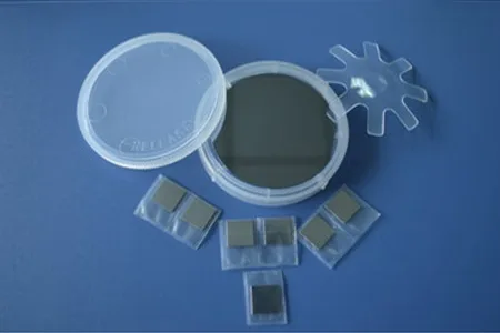
苏州科跃材料科技有限公司可提供各种规格、掺杂类型与晶向的磷化铟晶圆,支持科研与产业客户的定制需求,确保材料纯度高、晶体完整性强、缺陷密度低。


磷化铟晶圆物理性能

项目 参数说明
材料 InP(磷化铟)
生长方法 LEC、VGF
晶格常数(Å) a = 5.8687
晶体结构 锌矿结构(Zinc Blende)
熔点 1062°C
密度(g/cm³) 4.78 g/cm³
禁带宽度 1.34 eV(300 K,直接带隙)
折射率(@1.3μm) ~3.17
热导率 ~0.68 W/cm·K
导电类型 N型、P型、本征
掺杂元素 硫(S)、硒(Se)、锌(Zn)、铁(Fe)、未掺杂
迁移率 N型:3000–4500 cm²/V·s;P型:150–300 cm²/V·s

磷化铟晶圆技术规格

项目 参数范围
晶圆尺寸 10×10 mm、2″、3″、4″(支持定制)
厚度 350 µm、500 µm、600 µm(公差 ±25 µm)
表面处理 单面抛光(SSP)或双面抛光(DSP)
晶向 <100>、<111>
晶向偏差 ±0.5°
主定位边长度 22±2 mm、32.5±2 mm(按尺寸不同)
缺陷密度(EPD) ≤3×10⁴ cm⁻²(可选更低)
总厚度变化(TTV) <10 µm、<20 µm
翘曲度(Warp) <15 µm、<20 µm

包装方式

所有InP晶圆均在Class 1000洁净室中操作,并使用Class 100洁净袋或专用晶圆盒包装,确保表面洁净、无颗粒污染,满足精密器件制程要求。

评价

目前还没有评价

成为第一个“磷化铟晶圆” 的评价者

您的邮箱地址不会被公开。 必填项已用 * 标注

常见问题

Sputtering targets are materials used in thin-film deposition processes to create coatings on substrates. They are used in industries like semiconductors, optics, photovoltaics, and electronics.

Evaporation materials are used in Physical Vapor Deposition (PVD) processes, where materials are heated and evaporated to form a thin film on a substrate. These are critical for applications in optics, wear protection, and decorative coatings.

Boat crucibles are used as containers for evaporation materials during PVD processes. They help to uniformly evaporate materials onto the substrate for thin film formation.

Sputtering uses energetic particles to eject material from a target, while evaporation involves heating a material until it vaporizes and deposits on a substrate. Both are common methods in Physical Vapor Deposition (PVD) for creating thin films.

Consider the material composition, purity, target size, and application-specific requirements such as the thickness and uniformity of the film.

Yes, we offer customized sputtering targets, evaporation materials, and crucibles to meet specific customer requirements for size, material composition, and purity.

Yes, we can assist in selecting the most suitable material based on your application, whether it’s for optical coatings, semiconductor fabrication, or decorative finishes.

Yes, we offer both bulk and small quantities of sputtering targets, evaporation materials, and spherical powders to support research, prototyping, and development projects.