热氧化硅晶圆

热氧化硅晶圆在硅基底表面生长一层高质量二氧化硅绝缘层,广泛应用于微电子、MEMS、光电子器件中的栅介质、隔离层及掩膜层工艺。

描述

热氧化硅晶圆(Thermal Oxide Silicon Wafer)

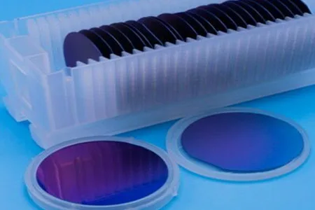
热氧化硅晶圆是在高温条件下,通过干氧或湿氧对硅晶圆进行热处理而形成的二氧化硅(SiO₂)绝缘层,是集成电路制造、微电子加工、MEMS器件和光电子元件中的关键基础材料。该氧化层具备优异的电绝缘性、热稳定性和界面质量,广泛用于栅介质、场区隔离、光掩膜层以及薄膜沉积工艺中的底层结构。

苏州科跃材料科技有限公司可提供各类厚度、导电类型和晶向的热氧化硅晶圆,支持干法氧化和湿法氧化两种工艺,满足科研与产业多样化需求。


热氧化硅晶圆技术规格

项目 参数说明
基底材质 单晶硅(Si)
晶圆尺寸 2″、3″、4″、6″、8″、12″(支持定制)
厚度 275–775 µm(视尺寸而定)
晶向 <100>、<111>、<110>
导电类型 N型、P型、本征
掺杂类型 磷(P)、硼(B)、锑(Sb)、砷(As)、无掺杂
表面处理 单面抛光(SSP)或双面抛光(DSP)
氧化层厚度(SiO₂) 50 Å – 10 µm(可选)
氧化方式 干氧化(Dry)或湿氧化(Wet)
氧化层均匀性 <±5%(可选更高等级)
TTV(总厚度变化) <10 µm、<20 µm
表面粗糙度(Ra) ≤5 Å(5 µm × 5 µm区域内)

热氧化方式对比简述

工艺方式 氧化速率 介电强度 应用场景
干氧化 慢,控制精准 更高 栅氧层、界面质量要求高场合
湿氧化 快,成本较低 稍低 隔离层、掩膜层、光刻辅助层等

包装方式

所有热氧化硅晶圆均在Class 1000洁净环境中处理,使用晶圆专用盒(FOUP/Cassette)或Class 100洁净袋封装,防静电、防颗粒污染,适合直接进入洁净工艺环境使用。

评价

目前还没有评价

成为第一个“热氧化硅晶圆” 的评价者

您的邮箱地址不会被公开。 必填项已用 * 标注

常见问题

Sputtering targets are materials used in thin-film deposition processes to create coatings on substrates. They are used in industries like semiconductors, optics, photovoltaics, and electronics.

Evaporation materials are used in Physical Vapor Deposition (PVD) processes, where materials are heated and evaporated to form a thin film on a substrate. These are critical for applications in optics, wear protection, and decorative coatings.

Boat crucibles are used as containers for evaporation materials during PVD processes. They help to uniformly evaporate materials onto the substrate for thin film formation.

Sputtering uses energetic particles to eject material from a target, while evaporation involves heating a material until it vaporizes and deposits on a substrate. Both are common methods in Physical Vapor Deposition (PVD) for creating thin films.

Consider the material composition, purity, target size, and application-specific requirements such as the thickness and uniformity of the film.

Yes, we offer customized sputtering targets, evaporation materials, and crucibles to meet specific customer requirements for size, material composition, and purity.

Yes, we can assist in selecting the most suitable material based on your application, whether it’s for optical coatings, semiconductor fabrication, or decorative finishes.

Yes, we offer both bulk and small quantities of sputtering targets, evaporation materials, and spherical powders to support research, prototyping, and development projects.